Select a Country or Region

2020-09-01

1: The basis for the selection of printed wire width: The minimum width of the printed wire is related to the size of the current flowing through the wire: the line width is too small, the resistance of the printed wire is large, the voltage drop on the line is also large, which affects the performance of the circuit, and the line width is too large. Wider, the wiring density is not high, the board area increases, in addition to increasing the cost, it is also not conducive to miniaturization. If the current load is calculated at 20A/mm2, when the thickness of the copper clad foil is 0.5MM, (usually so much), the current load of the 1MM (about 40MIL) line width is 1A, so the line width is 1-2.54 MM (40-100MIL) can meet the general application requirements. The ground wire and power supply on the high-power equipment board can be appropriately increased according to the power level. On the low-power digital circuit, in order to increase the wiring density, the minimum The line width is 0.254-1.27MM (10-15MIL) can be satisfied. In the same circuit board, the power cord. The ground wire is thicker than the signal wire.

2: Line spacing: When it is 1.5MM (about 60MIL), the insulation resistance between lines is greater than 20M ohms, and the maximum withstand voltage between lines can reach 300V. When the line spacing is 1MM (40MIL), the maximum withstand voltage between lines is 200V Therefore, on the circuit board of medium and low voltage (line-to-line voltage is not greater than 200V), the line spacing is 1.0——1.5MM (40——60MIL). In low-voltage circuits, such as digital circuit systems, it is not necessary to consider the breakdown voltage, as long as The production process permits and can be small.

3: Pad: For 1/8W resistance, the diameter of the pad lead is 28MIL, and for 1/2W, the diameter is 32MIL, the lead hole is too large, and the width of the pad copper ring is relatively reduced , Resulting in decreased adhesion of the pad. It is easy to fall off, the lead hole is too small, and the component is difficult to broadcast.

4: Draw the circuit frame: the shortest distance between the frame line and the component pin pad should not be less than 2MM, (usually 5MM is more reasonable) otherwise it will be difficult to blank.

5: Component layout principles: A: General principles: In PCB design, if the circuit system has both digital circuits and analog circuits. As well as high-current circuits, the layout must be separated to minimize the coupling between systems. In the same type of circuit, components are placed in blocks and partitions according to signal flow and function.

6: Input signal processing unit, output signal drive components should be close to the side of the circuit board, make the input and output signal lines as short as possible to reduce the interference of input and output.

7: Component placement direction: components can only be arranged in two directions, horizontal and vertical. Otherwise not for plug-ins.

8: Component spacing. For medium-density boards, small components such as low-power resistors, capacitors, diodes, and other discrete components are related to the plug-in and soldering process. When wave soldering, the component spacing can be 50-100MIL (1.27—2.54MM). Larger, such as 100MIL, integrated circuit chip, the component spacing is generally 100-150MIL.

9: When the potential difference between the components is large, the component spacing should be large enough to prevent discharge.

10: In the IC, the lotus coupling capacitor should be close to the power supply and ground pin of the chip. Otherwise, the filtering effect will be worse. In the digital circuit, in order to ensure the reliable operation of the digital circuit system, an IC decoupling capacitor is placed between the power supply and the ground of each digital integrated circuit chip. Decoupling capacitors generally use ceramic capacitors with a capacity of 0.01~0.1UF. The selection of decoupling capacitor capacity is generally selected according to the reciprocal of the system operating frequency F. In addition, a 10UF capacitor and a 0.01UF ceramic capacitor should be added between the power line and the ground line at the entrance of the circuit power supply.

11: The clock circuit components should be as close as possible to the clock signal pins of the microcontroller chip to reduce the wiring length of the clock circuit. And it is best not to route the wires below.

Various Soldering Defects In SMT PCB Production | SunzonTech

Production Line

Message

Shenzhen Sunzon Technology Co., Ltd.
+86 13417069748
+86-755-27307103
sales@sunzontech.com
Building 45, Hengkeng Industrial Zone, Genzhuyuan Community, Matian Street, Guangming District, Shenzhen, China
Philippine Branch:
+63 9178891559
ph-sales01@sunzontech.com

Contact

Shenzhen SunzonTech Co., Ltd

+86 0755 27357103
+86 13417069748
Building 45, Hengkeng Industrial Zone, Genzhuyuan Community, Matian Street, Guangming District, Shenzhen, China

Company

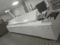
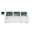
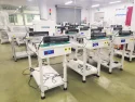
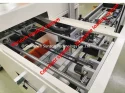
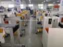
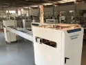
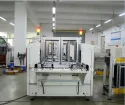
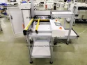
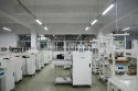
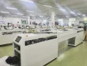
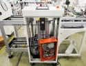
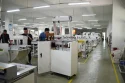
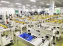
SunzonTech is a leading SMT (surface mount technology) machine supplier and SMT machine manufacturers in China. We have 17 years experienced in SMT machine design, R&D, manufacture and export.

We can also provide professional advice to establish a full SMT production line, as we have a rich of knowledge in the surface mount technology industry