2020-09-04
1. Electronic Components
Electronic components are the basic components of flexible electronic products, including thin film transistors and sensors commonly used in electronic technology. There is no essential difference between these electronic components and components of traditional electronic technology. Some components use inorganic semiconductor materials (such as silicon). Because their materials are brittle and are prone to brittle fracture during deformation, they are usually not directly distributed in the circuit. On the board, it is first placed on the rigid cell island, and then the cell islands that carry the components are distributed on the flexible substrate. The advantage of this is that it is beneficial to protect the electronic components and avoid them. Damaged during bending. Of course, some electronic components can also be directly distributed on the flexible substrate, for example, some thin film transistors, due to their own characteristics, can directly bear a certain strain without affecting their functions.
Compared with traditional microelectronics technology, in flexible electronic technology, the use of organic electronic components is a significant feature. Among them, organic thin film transistors occupy a very important position. The use of organic materials is to reduce the weight and thickness of components. Improve its flexibility and ductility to create conditions.
2. Flexible substrate
The flexible substrate is the most prominent place where flexible electronic technology is different from traditional electronic technology. It has the common characteristics of traditional rigid substrates. First of all, it is insulation: the insulated flexible substrate ensures that the electronic equipment will not leak during the use process, which not only ensures that it can work normally, but also ensures the safety of its use. The second is higher strength: no matter what kind of electronic technology, the role of the substrate is equivalent to the role of the skeleton, without higher strength as a guarantee, its normal use cannot be guaranteed.
The third is cheapness: the substrate material is one of the most used materials in circuits, and only the use of low-priced materials can effectively reduce the cost of electronic products.
In addition to the common features of the above-mentioned substrates, flexible substrates have their own unique characteristics. The first is flexibility: the flexibility of a flexible electronic system is mainly manifested by the substrate. Products with different requirements for flexibility can use substrates of different materials; for example, electronic skins usually use very flexible silicone resin (Silicone), while flexible Electronic displays have weaker requirements for flexibility than electronic skins, and most use polyethylene terephthalate material (PET), commonly known as polyester.
The second is thin film: Although it is called a substrate, its size is no longer a "board" but a thin film; the substrate of a flexible electronic system is usually about 1 mm, which reduces the cost of materials and reduces the cost of the product. weight.
In view of the above considerations, the use of high molecular polymers for flexible substrates is an ideal choice. The currently available flexible substrate materials include DuPont’s Kapton polyimide (Polyimide, PI) film materials, polydimethylsiloxane, polyethylene terephthalate (PET), etc., all of them It can well meet the requirements of insulation, flexibility and strength.
3. Cross-linked conductor
The electronic components are first distributed on the rigid microcell islands, and many of these microcell islands are then distributed on the flexible substrate. These microcell islands do not exist independently, they are connected by cross-linked conductors to form A complete flexible circuit, that is to say, the cross-linked conductors play the role of wires in the flexible electronic system. The cross-linked conductor is attached to the flexible substrate in the form of a metal thin film.
4. Adhesive layer
The combination of various components of the flexible electronic system requires an adhesive layer, and the adhesive layer is particularly important for the combination of cross-linked conductors and flexible substrates. The adhesive layer of the flexible electronic system should have the following characteristics:
(1) Heat resistance. In the process of assembly and use of flexible electronic products, it is inevitable to experience an environment higher than normal temperature, and certain heat resistance is necessary.
(2) Cohesion. Since flexible electronic products have to continuously undergo tension, compression, bending and deformation during use, and the two thin layers connected by the adhesive layer usually have different mechanical properties, if the bonding force is not large enough, it will inevitably lead to the relative sliding of the two thin layers or even Peel off.
(3) Bending ability. The adhesive layer itself is a component of the flexible electronic system structure, and its own bending ability has an important influence on the bending ability of the entire structure. At present, the commonly used adhesive layer materials in flexible circuits mainly include acrylic resin and epoxy resin.
5. Overlay
The cover layer (also known as the encapsulation layer) mainly protects the flexible circuit from dust, moisture or chemicals, and can also reduce the strain on the circuit during the bending process. Recent studies have shown that the cover layer can reduce the The stress intensity of the edge of the rigid microcell island (fcellisland), and can inhibit its delamination from the flexible substrate.
According to the characteristics of flexible electronic systems, the cover layer needs to be able to withstand long-term deflection. Therefore, the cover layer material is the same as the substrate material, and the fatigue resistance must meet certain requirements. In addition, the cover layer covers the sub-etched circuit, so it is required to have good conformability to meet the requirements of bubble-free lamination. Commonly used materials for the cover layer are acrylic resin, epoxy resin, and polyimide.
Manufacturing process of flexible electronic system
Like traditional IC technology, manufacturing processes and equipment are also the main driving forces for the development of flexible electronic technology. The technical level indicators of flexible electronics manufacturing include chip feature size and substrate area. The key is how to manufacture flexible electronic devices with smaller feature sizes on a larger-format substrate at a lower cost.
The flexible electronics manufacturing process usually includes: material preparation→deposition→patterning→encapsulation, which can be integrated through roll-to-roll (R2R) substrate transportation.
Flexible electronics manufacturing mainly focuses on factors such as production cost, production efficiency, achievable feature size, and compatibility of organic materials. In recent years, due to breakthroughs in active materials and their patterning technology, flexible electronics manufacturing technology has made considerable progress.
The core of flexible electronics manufacturing is thin film transistor (TFT) manufacturing, and its key manufacturing technology is to make high-resolution patterning technology for the channel length between source and drain, which directly affects the output current, switching speed and other device performance. In the organic semiconductor patterning process, it is particularly necessary to eliminate parasitic leakage and reduce crosstalk to ensure a high switching ratio. Most applications require organic thin film transistor (OTFT) channel lengths of less than 10 microns. Existing patterning techniques include photolithography, shadow mask, and printing (micro-contact printing and jet printing).
Energy beam technologies such as photolithography are widely used in the patterning of microelectronic devices, with high resolution. However, due to the complex process, expensive equipment, solvents and developers that cannot be used for plastic substrates, and time-consuming and material-consuming materials, they are only suitable for Small-area patterning requires harsh environments when etching the bottom layer, and when removing the photoresist, it will destroy the activity of organic electronic materials and polymer substrates, which is limited in flexible electronic manufacturing applications.
The shadow mask technology is a "dry" process, which can avoid solvent damage to organic semiconductors, but the resolution is limited.
Printing technology can realize functional material deposition and patterning at the same time in the same step. The main methods are: (1) Transfer and paste the complete circuit onto the flexible substrate, such as transfer printing (stamp); (2) Directly on the flexible substrate Preparation of circuits, such as jet printing and micro-contact printing (soft etching).
In the traditional printing method, the entire structure is first prepared on a silicon wafer or glass plate by a standard photolithography method, and then transferred to a flexible substrate to manufacture high-performance devices. Due to the application of photolithography and high-temperature deposition technology, the transfer printing technology can only manufacture small-area devices, and the processing cost is high.
Micro-contact printing can produce multi-level patterns for masks, which can be integrated with R2R batch manufacturing technology. Usually a master can produce more than 100 stamps, and each stamp can achieve more than 3000 imprints. The cost of the stamp is relatively low. It can produce 60nm high-resolution patterns at a speed of several centimeters per second, but realizes multi-layer patterns. more difficult. Micro-contact printing can be used for a variety of materials such as amorphous silicon, polysilicon and TMOS, but it is difficult to directly use organic materials for etching. Lan Hongbo and others discussed and analyzed the research progress and development trend of nanoimprint and etching mold technology in detail.
The ideal patterning process for flexible electronics should meet: low cost, large area, batch process, low temperature, "additive", non-contact, real-time adjustment, three-dimensional structure, easy multi-layer registration, printable organic/inorganic Materials, etc. Jet printing is a non-contact, pressure-free and plate-less printing and copying technology. It has the characteristics of plateless digital printing. The solution is directly written at room temperature to achieve digital flexible printing, which simplifies the manufacturing process. Using solutionized semiconductor and metal materials to replace traditional vacuum deposition materials can effectively reduce costs. Jet printing also has the following advantages:
(1) The quality of the pattern is not limited by the focal length of lithography, and it can be patterned on non-planar surfaces or even deep groove structures;
(2) Good compatibility with organic/inorganic materials;
(3) Directly use CAD/CAM data to process the device, which can realize large-area dynamic alignment and real-time adjustment;
(4) As a non-contact patterning technology, it can effectively reduce defects, and can use virtual masks to compensate for interlayer deformation, misalignment and other defects;
(5) Print on demand (DOD) technology without physical mask;
(6) The rapid design and processing of complex three-dimensional microstructures can be realized, and the graphics can be quickly changed through the software-based printing control system.
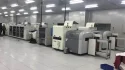
Short introduction of Panasonic NPM pick and place machine | SunzonTech
Various Soldering Defects In SMT PCB Production | SunzonTech
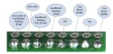
Categories
Title with button
this is a new beginning
We provide all your needed for starting your own online business, and even easier. Establish an online store, Oceans of Products Supply, Integrate Logistics Solution & Comprehensive After-sale Services.